
Imagine a world where you only need to charge your phone just once a month, or better yet, never, at least via a cumbersome cable. Imagine smart phones wirelessly charging effortlessly and continuously as you move about your home or office. Imagine a world where your smart phone ‘concierge’ asks you whether you would like to have your favorite hotel booked for your upcoming conference next week (yes, you forgot to book it). Indeed, we love ‘automation’ but for such science fiction to become a reality, a paradigm shift in AI hardware, chips, and associated services will need to come first. Talk to ECE’s Dr. Volker Sorger for more than five minutes and it becomes clear that he is already ‘living’ in that fantasy world—he’s just trying to get the rest of us there as well.

“The time is now—FSI, UF, and Florida are ready to lead the nation in next generation semiconductors and chip technology for the many applications and services that we enjoy and rely on every day. Full Speed Ahead!” –Dr. Volger Sorger
Dr. Sorger has quite a few titles in his email signature, belying his many leadership positions and responsibilities. He is the Walden and Paula Rhines Endowed Professor in Semiconductor Photonics in the Department of Electrical and Computer Engineering, director of the newly minted Florida Semiconductor Institute, theme lead for the SRC/DARPA JUMP 2.0 CHIMES Center, and task lead for the AFRL ExPlor Center. Prior to his arrival at the University of Florida, Dr. Sorger was a professor at the Department of Electrical and Computer Engineering at George Washington University. And, as his LinkedIn profile attests, Dr. Sorger was also a finalist to be an astronaut for the European Space Agency. Behind all these lofty titles is an unswayable passion and determination to make the semiconductor devices and chips at the heart our technology better, faster, and above all, more energy efficient.
Power-Hungry Computing
As he’s quick to point out, while the creation of the marvel we call ‘internet’ has transformed humanity’s access to information, its operation and recently added functionality (AI) are creating unprecedented demands for computational resources. Global data networks consume 200TWh today, or about one percent of all power consumed by humans. For countries like the U.S., the figure is more like ten percent. That may not seem like much, but the issue is the current rate of growth. According to Dr. Sorger, if we continue with ‘compute-as-usual’ hardware solutions, within a decade, all available power will be consumed by our computing infrastructure. The path we’re on is unsustainable, and to Dr. Sorger, some of the bottlenecks are obvious—limited access to memory and incomplete solutions for packaging of heterogeneous chips.
At the heart of our AI-powered world is powerful semiconductor-filled hardware executing machine-learning algorithms; ChatGPT comes to mind for the latter, and NVIDIA’s powerful GPUs for the former. The current wave of AI technology is driven by a hardware innovations. So, given the unsustainable power scaling and our desire for more task automation, what performance and capabilities should future semiconductor chips have? These are questions Dr. Sorger and the Florida Semiconductor Institute are exploring.
Next-generation AI computation solutions will need to meet two requirements. They will require tremendous amounts of computer memory, and they should be designed with brain-inspired design concepts, rather than today’s brute-force compute systems. Emerging solutions currently include concepts such as a compute-in-memory (where the memory is co-located near the processor) or high-bandwidth-memory. However, such solutions are constrained by design spaces given by capacitance, energy requirements, voltage regulation, and heat dissipation.
A solution proposed and demonstrated in a recently released article by Dr. Sorger and his FSI team, together with collaborators, is to use the best-of-all-worlds—optics combined with electronics. Many are familiar with fiber optic connections for home internet, offering highest data-rate speeds. And electronic solutions are able to store information well. Dr. Sorger’s team showed that photonic-electronic hybrid circuits could be built that would create a revolutionary kind of photonic memory.
Thanks for the Memory
Most are familiar with the little memory chips that are part of our computers. They are the answer to the question, “how much RAM is in your machine?” Memory, or RAM (random access memory), functions as the work area for our computing devices, where calculations are made, instructions interpreted and executed. As RAM is traditionally adjacent to, not part of, the central processing core, every calculation involves some data movement from CPU to memory and back again. It is this tiny voyage which can be transformed by the ground-breaking technology. In photonic memory devices, the data moving between the processor core(s) and the memory modules travels not through wires electrically, but as light inside on-chip waveguides. Also known as optical or photonic RAM (or short ‘PRAM’), these chips perform calculations in the optical domain, offering faster and higher energy efficiency by potentially up to a factor of 100, while offering electronic data storage at the same time. The technology is poised to revolutionize computing at its core.
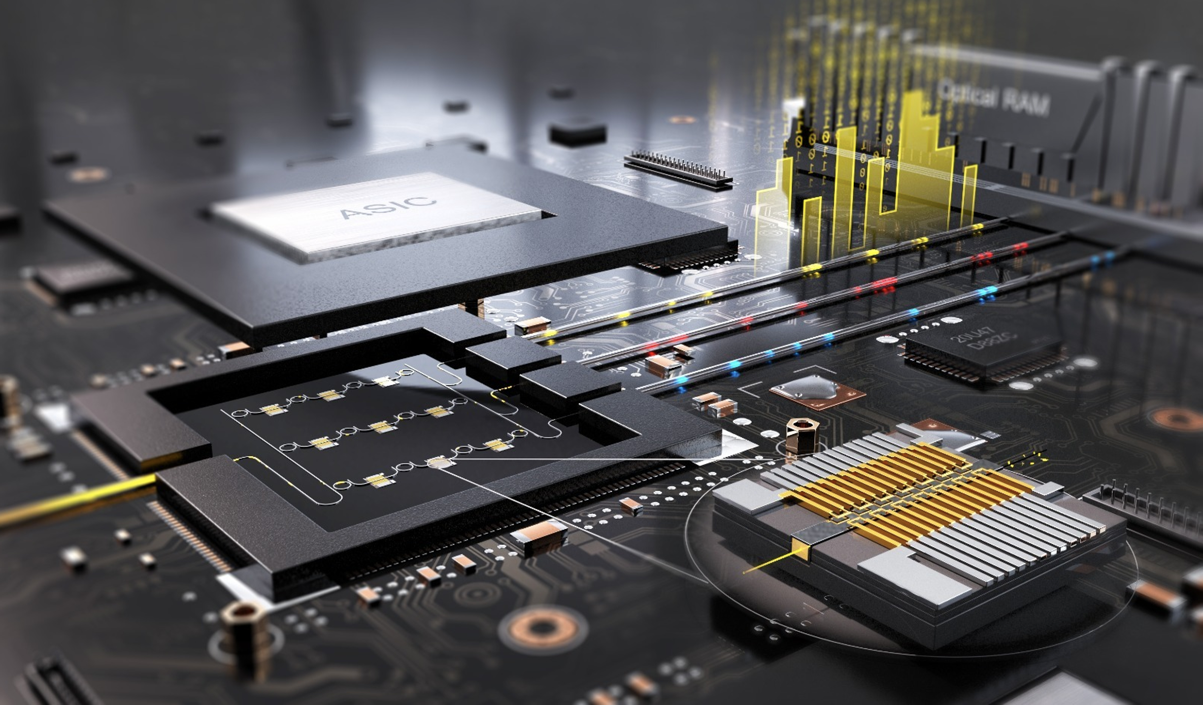
Photonic Memory Cells
The physics and engineering behind PRAM cells are wildly complex. One critical detail built into this technology is the fact that the memory cells are made of phase-change materials. The light traveling on nanoscopic waveguides and interacting with this phase-change material ‘touching’ the waveguide causes the light to be ‘switched,’ thus carrying the stored information from the memory element inside the photonic-electronic processor. The phase change material itself can be switched between two structural states, amorphous and crystalline states, with distinct optical and electrical properties, for memory programability. As Dr. Sorger says, the light present in the devices actually causes the material to behave as a memory chip. Read the full article at the Nature Light Science & Applications website.
One area in which photonics memory shows great potential is in national security and defense. Dr. Sorger is the principal investigator on a 3-year $3M grant from the Office of Naval Research Electronic Warfare Program. Collaborating with ECE researchers Dr. David Arnold, Dr. Navid Asadi, Dr. Bhaibab Chatterjee, Dr. Hamed Dalir, as well as colleagues from UCLA, the project, ‘Heterogenous Convolution ASIC for AI Acceleration (HelCat),’ will develop an electronic-photonic processor that can deliver leading-edge performance for next-generation machine learning and signal processing capabilities used in mission-critical defense equipment and infrastructure.
While the horizons may not be endless, the realm of photonics certainly holds immense promise. Dr. Sorger’s passion and leadership, coupled with the resources and network afforded to the Florida Semiconductor Institute, could very well pave the way to the very future he envisions—a world characterized by enhanced speed, energy efficiency, and superior technology. So, as we stand at this precipice of innovation, it’s evident that the path ahead is illuminated with hope and the potential to bring about transformative change.
Florida Semiconductor Institute
Finalized in the summer of 2023, the Florida Semiconductor Institute (FSI) was created to focus on regional leadership in the semiconductor research and development space, to attract federal and private funding, and to boost the nation’s semiconductor workforce. While Florida boasts the fifth-largest semiconductor workforce in the U.S. and offers next generation chip packaging corporations and major electronics manufactures design offices (similar to California), Florida currently lacks large-volume chip manufacturing foundries that can fully leverage the talent pipeline. FSI aims to harness UF’s community of interdisciplinary researchers to accelerate the ‘lab-to-fab’ pipeline.
It is estimated that the future of semiconductor manufacturing will require the doubling of the domestic semiconductor workforce in one decade, according to Dr. Sorger and supported by the U.S. CHIPS and Science Act from 2022. In response, the institute’s mission is to: 1) drive research and innovation forward with a focus on AI chips and heterogeneous chip solutions, 2) support the onshoring of semiconductor manufacturing with a focus advanced chip packaging, and 3) prepare and support a greatly expanded U.S. workforce in semiconductor manufacturing.