“Taming Material Noise in Superconducting Quantum Circuits”
Monday, Feb. 5 at 1:00pm
LAR 234
Add to Calendar
Abstract
Noise within solid-state systems at low temperatures, where many of the degrees of freedom of the host material are frozen out, can typically be traced back to atomic-scale material defects that support low-energy excitations, commonly described by the tunneling two-level systems (TLS) model. Although the details of TLS and their impact on the low-temperature behavior of materials have been studied since the 1970s, these states have recently taken on further relevance in the field of quantum computing, where the limits to the coherence of superconducting quantum circuits are dominated by TLS. Efforts to mitigate the impact of TLS have thus far focused on circuit design, material selection, and material surface treatment.
In this talk, I will present a new approach that seeks to directly modify the properties of TLS through nanoscale engineering. In the first part of the talk, I will introduce a hybrid experimental platform that integrates a transmon qubit hosting a sparse bath of TLS within a tailored acoustic structure. The acoustic structure features a GHz-wide acoustic bandgap at the operating frequency of a transmon qubit, which suppresses all microwave-frequency phonons and effectively shields embedded TLS from direct phonon emissions when the TLS transition frequency lies within the acoustic bandgap. Beyond the microwave-frequency noises associated with these TLS, solid-state materials generally exhibit low-frequency noises that are responsible for qubit dephasing. In the second part of the talk, I will discuss the detection and control of individual thermally-activated TLS with resonance frequencies in the MHz range. I will also discuss the implications of these findings for understanding and mitigating 1/f-like noise in solid-state materials.
Biography
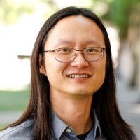
Mo Chen is a postdoctoral scholar in Professor Oskar Painter’s group at the California Institute of Technology, where he has pioneered the engineering of material defects in superconducting quantum circuits. Prior to this, he received his B.S. in Optics from Fudan University in 2012 and his S.M. and Ph.D. in Mechanical Engineering from MIT in 2015 and 2020, respectively. His research, employing tools like quantum sensing, quantum control, and nanoscale engineering, focuses on developing a deep understanding of device physics, for both fundamental explorations and practical applications in quantum information science.

